- 您现在的位置:买卖IC网 > Sheet目录1194 > ADL5315-EVAL (Analog Devices Inc)BOARD EVAL FOR ADL5315
�� ��
��
��ADL5315�
�THEORY� OF� OPERATION�
�The� ADL5315� addresses� the� need� for� precision� high-side�
�monitoring� of� photodiode� current� in� fiber� optic� systems� and� is�
�useful� in� many� nonoptical� applications� as� well.� It� is� optimized�
�for� use� with� ADI’s� family� of� translinear� logarithmic� amplifiers,�
�which� take� advantage� of� the� wide� input� current� range� of� the�
�ADL5315.� This� arrangement� allows� the� anode� of� the� photo-�
�diode� to� connect� directly� to� a� transimpedance� amplifier� for� the�
�extraction� of� the� data� stream� without� the� need� for� a� separate�
�optical� power� monitoring� tap.� Figure� 19� shows� the� basic�
�connections� for� the� ADL5315.�
�ADL5315�
�The� ADL5315� provides� a� setpoint� reference� pin,� SREF,�
�which� can� be� connected� to� VSET� for� standard� 2-port�
�mirror� operation.� V� SREF� is� maintained� 1.0� V� below� V� POS� over�
�temperature� and� is� independent� of� input� current.� When� using�
�SREF� to� set� the� input� voltage,� a� capacitor� should� be� placed�
�between� SREF� and� ground� to� filter� noise� from� SREF� as� well�
�as� improve� power� supply� rejection� over� frequency.� A� value� of�
�2.2� nF,� for� example,� combined� with� the� 20� k� output� resistance�
�at� SREF,� creates� a� pole� at� approximately� 3� kHz.�
�The� voltage� at� the� SREF� pin� can� be� lowered� to� a� desired� fixed�
�value� with� the� use� of� a� single� external� resistor� from� SREF� to�
�4�
�COMM�
�RLIM� 5�
�R� LIM�
�ground.� Mismatch� between� on-chip� and� external� resistors�
�limits� the� accuracy� of� the� resultant� voltage.� In� addition,� internal�
�2.2nF�
�3�
�SREF�
�VPOS� 6�
�0.1� μ� F�
�0.01� μ� F�
�VOLTAGE�
�SUPPLY�
��shows� an� equivalent� circuit� model� of� the� SREF� biasing.� The�
�2�
�VSET�
�NC� 7�
�Schottky� diode� clamp� protects� the� 50� μA� current� source� when�
�4k� Ω�
�390pF�
�1�
�INPT�
�IOUT� 8�
�MIRROR�
�CURRENT�
�OUTPUT�
�SREF� is� pulled� to� ground.� When� V� SREF� is� 1.2� V� or� higher,� the�
�50� μA� current� flows� to� the� SREF� pin.� The� current� is� shunted�
�away� and� does� not� appear� at� the� SREF� pin� for� V� SREF� <� 0.6� V.�
�The� transition� region� is� between� 0.6� V� and� 1.2� V� with� a� large�
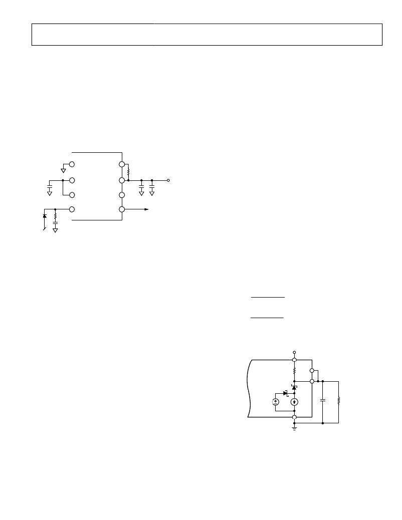
�Figure� 19.� Basic� Connections�
�At� the� heart� of� the� ADL5315� is� a� precision� 1:1� current�
�mirror� with� a� voltage� following� characteristic� that� provides� an�
�adjustable� bias� voltage� at� the� mirror� input.� This� architecture�
�uses� a� JFET� input� amplifier� to� drive� the� bipolar� mirror� and�
�maintain� stable� V� INPT� voltage,� while� offering� very� low� leakage�
�uncertainty� in� the� pull-down� current.� It� is� recommended� that� a�
�2-resistor� divider� from� VPOS� (with� no� connection� to� SREF)� or�
�another� external� bias� be� used� to� bias� VREF� in� this� transition�
�region.�
�Equations� for� the� SREF� voltage� with� an� external� pull-down� R� EXT�
�follow:�
�current� at� the� INPT� pin.� The� current� sourced� by� the� low�
�impedance� INPT� pin� is� mirrored� and� sourced� by� the� high�
�impedance� IOUT� pin.�
�V� SREF� =�
�R� EXT�
�R� EXT� +� 2� 0� k�
�(� V� POS� ?� 1� .� 0� V� )� ,� V� SREF� ≥� 1� .� 2� V�
�BIAS� CONTROL� INTERFACE�
�V� SREF� =�
�R� EXT�
�R� EXT� +� 2� 0� k�
�V� POS� ,� V� SREF� ≤� 0� .� 6� V�
�The� voltage� at� the� INPT� pin,� V� INPT� ,� is� forced� to� be� equal� to� the�
�voltage� applied� to� VSET� by� the� mirror-biasing� loop.� The� V� SET�
�voltage� range� extends� down� to� ground,� allowing� the� ADL5315�
�to� be� used� as� a� voltage-to-current� converter� with� a� single� resistor�
�where� the� 20� k� is� the� process-dependent� internal� resistor.�
�V� POS�
�from� INPT� to� ground.� This� capability� allows� dark� current� to� be�
�minimized� in� PIN� photodiode� systems� by� maintaining� a� small�
�ADL5315�
�20k� Ω�
�VSET�
�voltage� bias.� The� VSET� control� also� allows� V� INPT� to� be� set�
�approximately� equal� to� the� load� voltage� at� IOUT.� Balancing�
�the� mirror� voltages� in� this� way� provides� inherently� superior�
�SREF�
�linearity� over� the� widest� current� range� independent� of� the�
�0.9V�
�50� μ� A�
�C� SET�
�R� EXT�
�supply� voltage.� Only� leakage� currents� from� the� JFET� op� amp�
�and� ESD� devices� remain� as� significant� sources� of� nonlinearity�
�at� very� low� currents.� The� voltage� at� VSET� can� also� be� used� to�
�shield� the� highly� sensitive� INPT� pin� and� its� board� trace� from�
�leakage� currents,� because� the� two� pins� operate� at� approximately�
�the� same� potential.� Care� must� be� taken� to� provide� a� low� noise�
�V� SET� signal,� since� voltage� noise� at� VSET� also� appears� at� INPT�
�and� is� transformed� by� the� input� compensation� network� into�
�current� noise.�
�Rev.� 0� |� Page� 9� of� 20�
�Figure� 20.� Model� of� SREF� Bias� Source� with� External� Pull-Down�
�发布紧急采购,3分钟左右您将得到回复。
相关PDF资料
ADM00333
BOARD EVAL FOR PIC18F87J72
ADM00344
BOARD DEMO EVAL FOR RE46C190
ADM00345
BOARD DEMO 3PH BLDC CTLR MTD6505
ADM1026EBZEVB
BOARD EVAL FOR ADM1026
ADN8831-EVALZ
BOARD EVAL FOR ADN8831
ADP1043AFB100EVALZ
BOARD EVALUATION ADP1043A 100W
ADP1046-100-EVALZ
BOARD EVAL FOR ADP1046-100
ADP1048-600-EVALZ
BOARD EVAL ADP1048-600
相关代理商/技术参数
ADL5317
制造商:AD 制造商全称:Analog Devices 功能描述:Avalanche Photodiode Bias Controller and Wide Range (5 nA to 5 mA) Current Monitor
ADL5317ACPZ-REEL7
功能描述:IC CURRENT MONITOR 16LFCSP RoHS:是 类别:集成电路 (IC) >> PMIC - 稳流/电流管理 系列:- 产品培训模块:Lead (SnPb) Finish for COTS
Obsolescence Mitigation Program 标准包装:50 系列:- 功能:电流开关 检测方法:- 精确度:±10% 输入电压:1.7 V ~ 5.5 V 电流 - 输出:600mA 工作温度:-40°C ~ 125°C 安装类型:表面贴装 封装/外壳:10-UFQFN 供应商设备封装:10-UTQFN(1.4x1.8) 包装:管件
ADL5317ACPZ-WP
制造商:Analog Devices 功能描述:SP Amp LOG Amp Single 6V/80V 16-Pin LFCSP EP Tray 制造商:Analog Devices 功能描述:SP AMP LOG AMP SGL 6V/80V 16LFCSP EP - Bulk
ADL5317-EVAL
制造商:Analog Devices 功能描述:EVAL BD FOR AVALANCHE PHOTODIODE BIAS CNTRLR AND WIDE RANGE - Bulk
ADL531A-53M0
制造商:Panasonic Industrial Company 功能描述:VALVE
ADL5320
制造商:AD 制造商全称:Analog Devices 功能描述:400 MHz to 2700 MHz RF Driver Amplifier
ADL5320_08
制造商:AD 制造商全称:Analog Devices 功能描述:400 MHz to 2700 MHz RF Driver Amplifier
ADL5320ARKZ
制造商:Analog Devices 功能描述:AMP DVR RF 400MHZ-2.7GHZ 3SOT89 制造商:Analog Devices 功能描述:AMP, DVR, RF, 400MHZ-2.7GHZ, 3SOT89 制造商:Analog Devices 功能描述:AMP, DVR, RF, 400MHZ-2.7GHZ, 3SOT89; Frequency Min:400MHz; Frequency Max:2.7GHz; Gain:17dB; Noise Figure Typ:5.1dB; RF IC Case Style:SOT-89; No. of Pins:3; Supply Voltage Min:4.5V; Supply Voltage Max:5.5V; RF Type:Broadband; ;RoHS Compliant: Yes